At its annual Technology Symposium, semiconductor manufacturer TSMC detailed characteristics of its 5nm and 3nm processes which Apple is expected to use for its next generation processors.
The iPhone 12 will likely feature an A14 processor built on TSMC's 5nm processor. AnandTech reports that the N5 process node is progressing with defect densities one quarter ahead of N7 and with better yields at mass production than both N7 and N10.
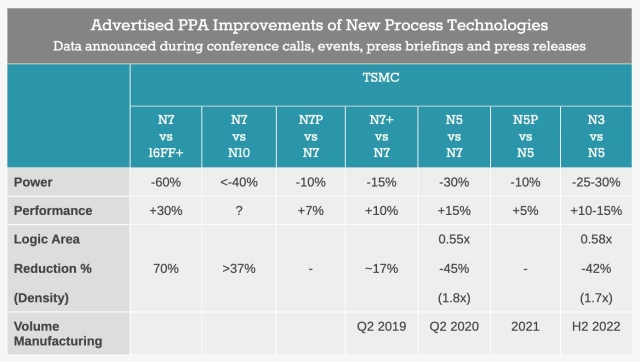
The N5 process offers either a 30% reduction in power usage or a 15% increase in speed, compared to N7. Apple will decide how to balance power and performance for its chips, likely choosing more performance over a significant reduction in power consumption.


Notably, in 2022, TSMC will launch its 3nm process which also offers a similar 25-30% reduction in power requirements or a 10-15% boost in performance over the 5nm process.
Today’s biggest news was TSMC’s disclosure on their next big leap past the N5 process node generation family, which is the 3nm N3 node. We’ve heard that TSMC had been working on defining the node back last year with progress going well. Contrary to Samsung’s 3nm process node which makes use of GAA (Gate-all-around) transistor structures, TSMC will instead be sticking with FinFET transistors and relying on “innovative features” to enable them to achieve the full-node scaling that N3 promises to bring.
More details in the full report linked below!
Read More


The iPhone 12 will likely feature an A14 processor built on TSMC's 5nm processor. AnandTech reports that the N5 process node is progressing with defect densities one quarter ahead of N7 and with better yields at mass production than both N7 and N10.
The N5 process offers either a 30% reduction in power usage or a 15% increase in speed, compared to N7. Apple will decide how to balance power and performance for its chips, likely choosing more performance over a significant reduction in power consumption.


Notably, in 2022, TSMC will launch its 3nm process which also offers a similar 25-30% reduction in power requirements or a 10-15% boost in performance over the 5nm process.
Today’s biggest news was TSMC’s disclosure on their next big leap past the N5 process node generation family, which is the 3nm N3 node. We’ve heard that TSMC had been working on defining the node back last year with progress going well. Contrary to Samsung’s 3nm process node which makes use of GAA (Gate-all-around) transistor structures, TSMC will instead be sticking with FinFET transistors and relying on “innovative features” to enable them to achieve the full-node scaling that N3 promises to bring.
More details in the full report linked below!
Read More


